Electrical Schematics and Design
Overall Schematic

MCU Circuits
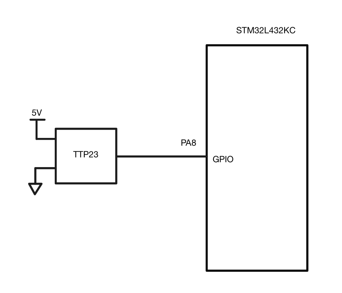
1. Capacitive Touch Sensor Circuit
The MCU uses a Capacitive Touch Sensor to detect a user’s hand to trigger the start of the whole sequence (Figure 2). The GPIO receives that signal on PA8 which simultaneously triggeres PA5 which is electrically connected to P47 to send a signal to the FPGA components as well.
The Capactive Touch Sensor receives 5V and ground from the circuit. It works by applying a small voltage to create a constant electrostatic field on one surface. When that conductive material is touched by a human, a capacitor is formed from the virtual ground that the user provides. This is seen in practically every smart device around us today.
We tested it by connecting to a multimeter to see the max voltage that could be received on the GPIO pin when detecting a finger touch.
One of the main difficulties with this sensor was integrating it mechanically as it had to be detectable through the 3D printed PLA that we used for Toothless. So there were many moments where we thought there was something going wrong on the electrical and software side when it was was the mechanical.
One thing that we did right before demo day was that the Capacitive Touch Sensor would randomly trigger when the dragon box was even touched. This is wherewe found that the make to femal connector that we placed into the GPIO pin would easily wiggle around causing the signal to flicker. So we replace it…stranded wire for the win.
2. IR Proximity Sensor Circuit
The MCU also deals with detecting hand placement into the mouth using an IR Proximity sensor. The sensor works by placing an IR LED and IR detector pair next to each other such that the IR detector takes the IR light that reflects off an object that comes near the top of the IR light (Figure 3). The closer the object, the stronger the IR intensity of the reflection.
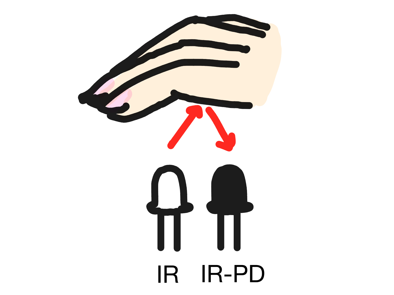
The circuit is heavily inspired by AutoDesk Instructuable’s Proximity Sensor, but without a potentiometer for changing the distance of the object away from the sensor that the circuit can detect. The circuit schematic is shown below (Figure 4). Note that the IR LED is in the opposite direction as the IR Photodetector (IR-PD).
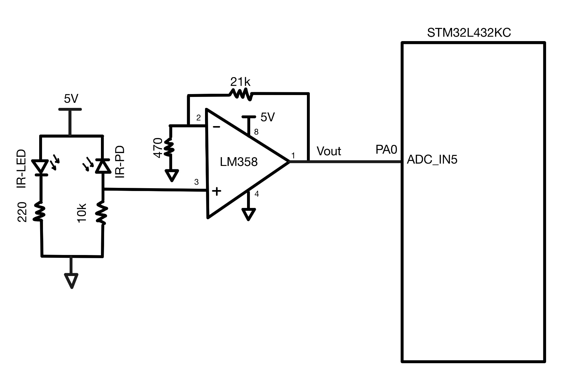
The more InfraRed light that falls on the IR-PD, the more current that flows through the PD. This current then flows through the 10kΩ resistor connecting the cathode of the PD to ground which increases the voltage potential across the resistor that is seen by the positive terminal of the LM358 op-amp (Pin 2). The op-amp is configured with a non-inverting gain based on the resistorconnected between vout and the negative terminal (R1) and the resistor connected between the negative terminal of the op-amp to ground (R2). The gain of the non-inverting op-amp (A) follows the equation below.
\[ A_{non-inverting} = 1 + \frac{R_{1}}{R_{2}} = 1 + \frac{21kΩ}{470Ω} = 44.7 \]
In Figure 4, because we used R1 = 21kΩ and R2=470Ω, the gain of our circuit was around 45. This allowed for a hand near the sensor to be detected but the roof of the mouth to not be detected when the jaw was open. For debugging the circuit, we recommend to place an LED in series with a resistor to ground at the voltage output of the op-amp. The LED brightness should increase as the object gets closer to the LED pair.
3. DFPlayer Mini Circuit
One of the big issues for the DFPlayer was that the RX and TX channels were swapped for the longest time. Although a seemingly simple mistake, it was one that tripped us up for a while because there wasn’t a proper datasheet to reference of each of the DFPlayers pin outs. Additionally the DFPlayer works on its own independently so if all your files are named and numbered correctly (which was also a big issue at first) you can use the ADKEY and IO ports to trigger play different segments on the TF card. It was unclear for a while whether it was recieving an electrical signal or what we were producing via the software’s UART signals.
The circuit itself is largely inspired by sample circuits on the Picaxe Datasheet that we later found as well as a MP3-TF-16p Tutorial on Youtube. The schematic for the DFPlayer mini is shown below (Figure 5)
Since the DFPlayer was completely controlled via the MCU no signal was sent to the FPGA.
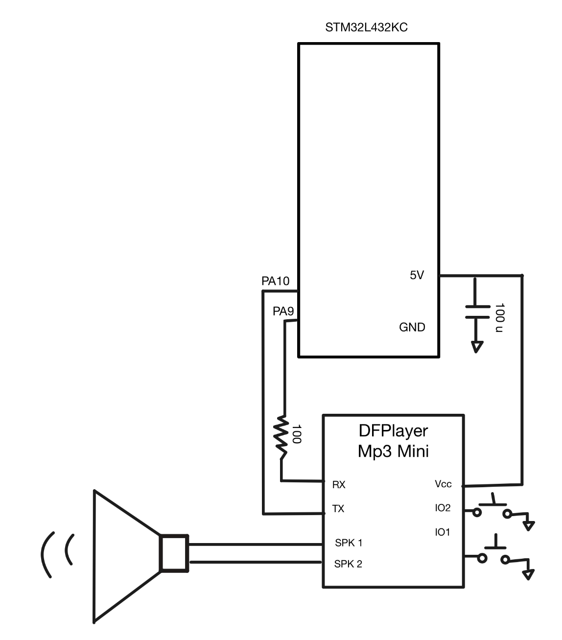
One big thing we learned was to use stranded wire for as many things as we can because the speaker and various connections often broke off without notice during the debugging process.
FPGA Circuits
1. Servo Motor Circuit
One issue we ran into was the power the servo motor drained when moving which caused the music on the DFPlayer mini to cut out when the servo was in action and meant that we couldn’t play music at the same time that the jaw opened. To circumvent this, we powered the servo motor with a 5V power supply separate from the 5V provided by the MCU. It is important to connect the ground of the servo and the ground of the power supply to the same ground as the MCU and FPGA such that they all share common ground. The issue of common ground ended up being a nasty and almost invisible problem that was hard to debug later when the circuit board and breadboard were hidden underneath our box stand.
Another way we ensured the servo inject noise into the MCU was using a non-inverting NPN open-collector buffer. This also allowed us to provde the servo with the necessary clean high and low signal for the PWM. The FPGA pins only supply 3.3V which has potential to muddle the PWM signal where the FPGA would see 3.3V as low rather than as high, thus using the two NPN transistor configuration created a non-inverting buffer that pulled the 3.3V signal to a 5V signal. The schematic for the non-inverting, two NPN buffer and servo motor is below (Figure 6).
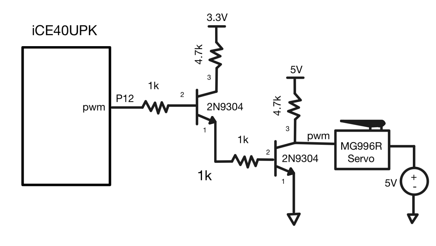
The 1kΩ resistor from the FPGA pin (P12) to the base of the NPN transistor protects the FPGA pin by limiting base current while the 4.7kΩ resistor acts as a pull-up resistor for the collector. We used 2N9304 transistors which has the emitter on Pin 1, the base on Pin 2, and the collector on Pin 3 (Figure 6). If using a different NPN transistor, be sure to check the transistor’s pinout.
2. LED Array Circuit
The LED array circuit (Figure 7) is simply 10 LEDs wired with a 1kΩ resistor in series to ground. The LED strip uses another 2N3904 NPN transistor that uses a signal from the FPGA to decided whether or not to turn the light strip on. We had to use a separate power supply that provided 12V as the 5V from the MCU and the 3.3V from the FPGA were too low to power the LED strip.

It is important to note that unlike the servo motor, the LED light strip is placed in series with the voltage source such that the cathode of the light strip is attached to the positive terminal of the power supply and the anode is connected to the collector (Pin 3) of the transistor. The resistor between the FPGA pin (P13) is greater than that for the servo as the voltage being supplied from the power supply is also much greater. When programming the LEDs, the order can be chosen based on which pins you send a high signal to first. For our purposes, we lighted in a certain order but placed the LEDs not in order to create a slightly random light show. See the software design section for more details.