Lab 2 Report
Lab Hours
I spent 20 hours on this lab.
Introduction
Lab 2 involved learning time multiplexing and application of PNP transistors to efficiently use the I/O on the FPGA by using one module and two 4 DIP switch inputs to control a dual 7-segment display on a breadboard. The lab also involved displaying the sum of the two inputs onto external LEDs.
Design and Testing Methodology
Dual Display with one 7-Segment Module
In order to display two independent hexadecimal numbers on the dual 7-segment display using only one sevseg module, the trick was to send the same output to both digits but alternate between turning on the first digit and the second digit fast enough that the different digits are seen at the same time to our eyes (~60 Hz). To alternate between the two, the on-board high-speed oscillator (HSOSC) from the iCE40 UltraPlus primitive library was used to generate a clock signal at 24 MHz then a counter was used to divide the high frequency clock signal into a 60 Hz signal.
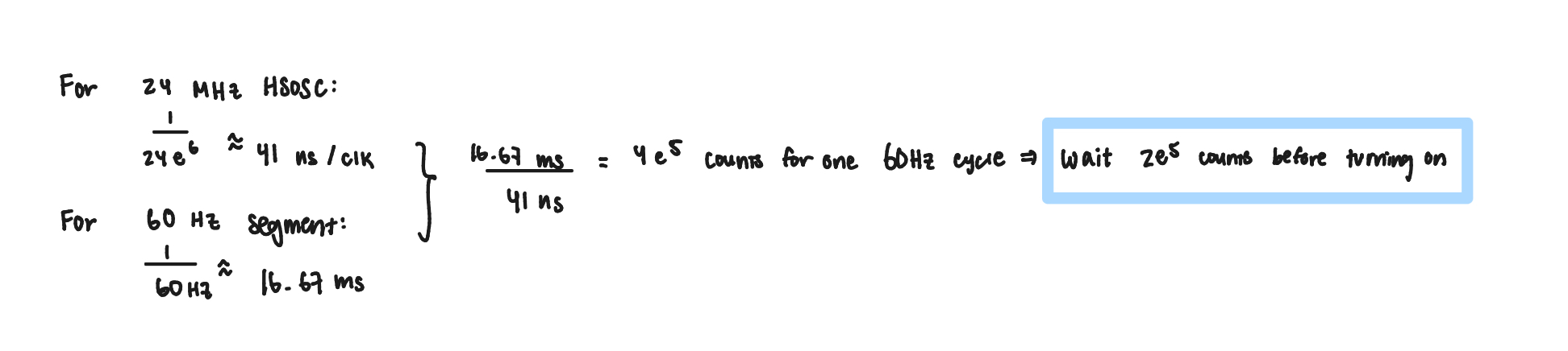
The calculation in Figure 1 derived that the counter needed to reach 200000 before setting the multiplexer select HIGH in order switch between the two inputs and turning on the two outputs at 60 Hz. For example, if the first digit should read 1 and then second digit should read 5, then when clk is LOW, the program takes 1 as the input and sends 1 to both digits’ outputs. Then, the program turns only the first digit’s power on and turns the other digit’s power off. When clk is HIGH, the program takes 5 as the input and sends 5 to both digits’ outputs. Then the program turns the second digit’s power on and turns the first digit’s power off. This switch happens fast enough that the human eye sees both individual digits on the display.
Resistor choice for 7-segment Display
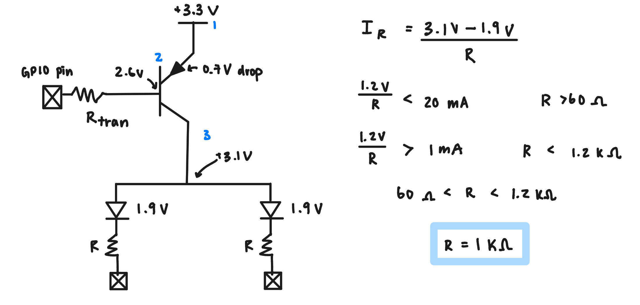
The calculation in Figure 2 derived 1kΩ as an appropriate resistor to provide ~1.2 mA to the LED segments of the 7-segment display. The drop in voltage from the emitter is due to the emitter saturation voltage. Thus the voltage going into the segment displays is 3.1 V.
Resistor choice for external LEDs
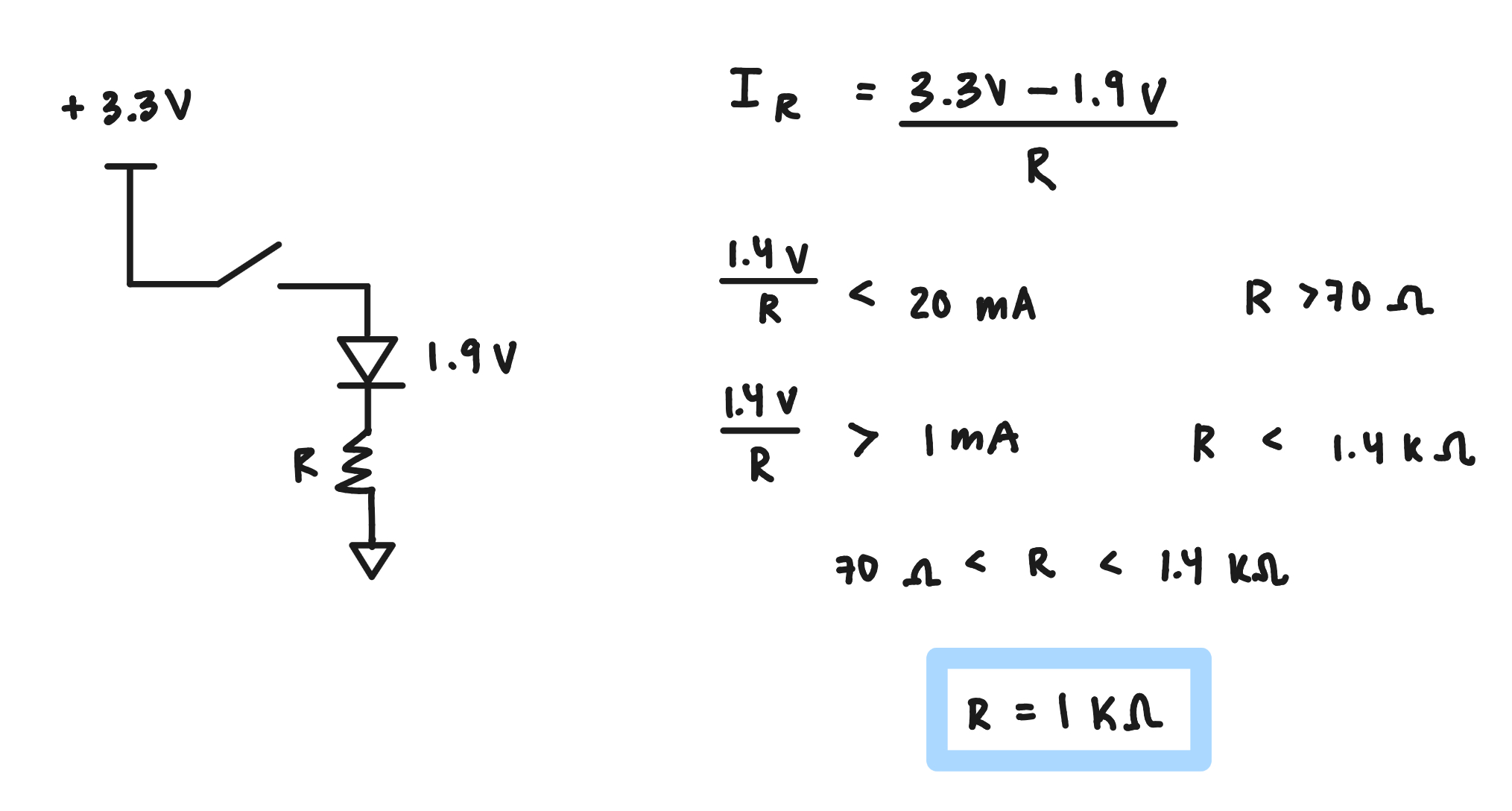
The calculation in Figure 3 derived 1kΩ as an appropriate resistor to provide ~1.4 mA to the external LEDs. The calculation is the same as for the 7-segment display, however the cathodes of the LEDs are connected to ground rather than to a pin.
Resistor choice for transistors
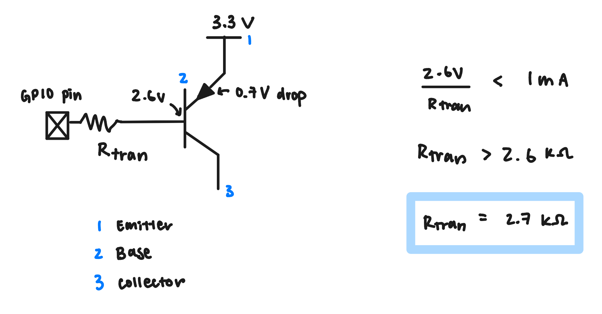
The calculation in Figure 4 derived 2.7kΩ as an appropriate resistor (stock-room available) to provide less than 1 mA to FPGA I/O pins.
Technical Documentation
The source code for the project can be found in the associated Github repository
Block Diagram
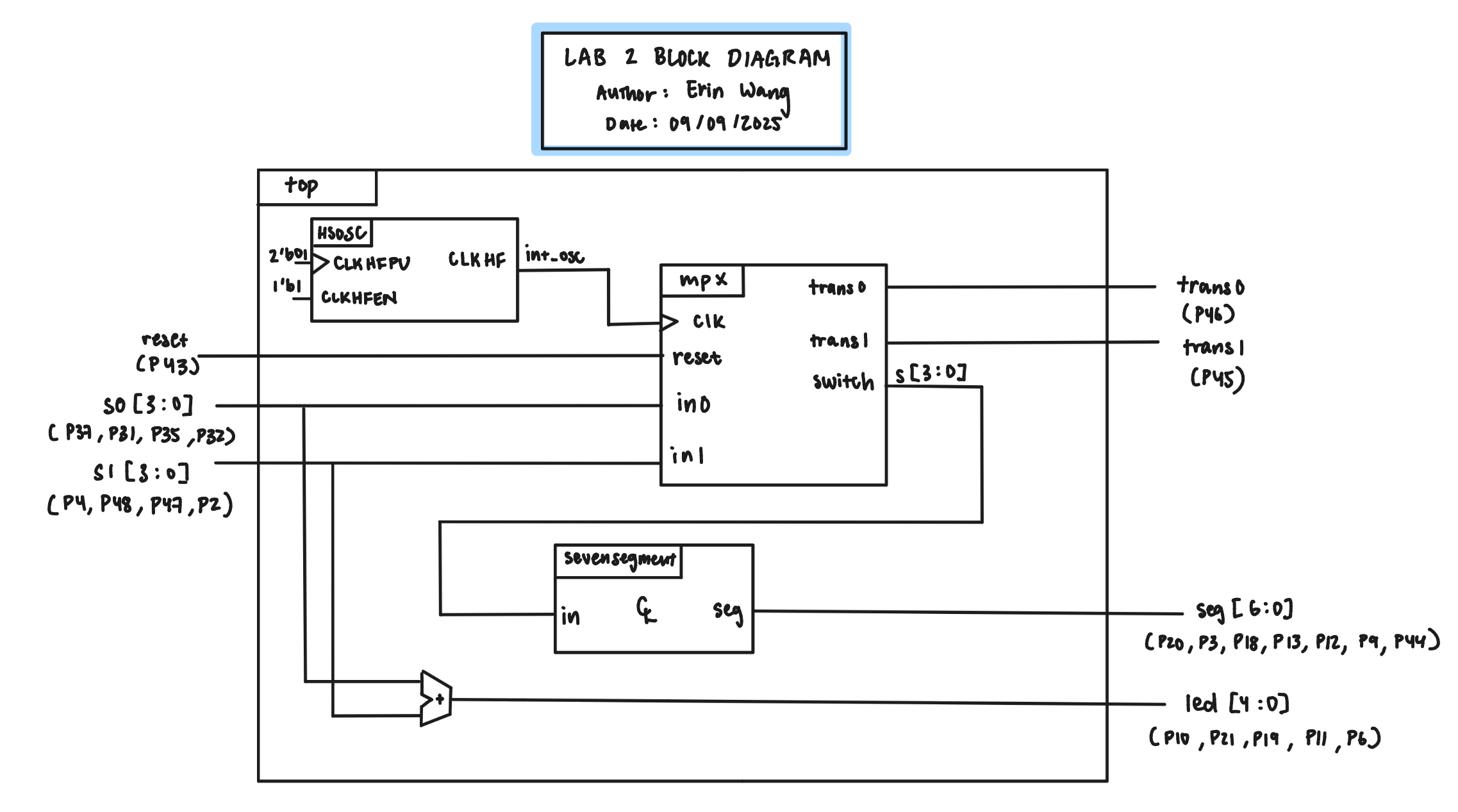
HSOSC, mpx, and sevseg.
The block diagram in Figure 5 demonstrates the overall architecture of the design. The top-level module top includes three submodules: the high-speed oscillator block (HSOSC), the multiplexer to alternate at 60 Hz (mpx), and the 7-segment display module from Lab 1 (sevseg). The programming for the LED sum and the multiplexer logic using the select output of mpx were placed in the top module.
Schematic
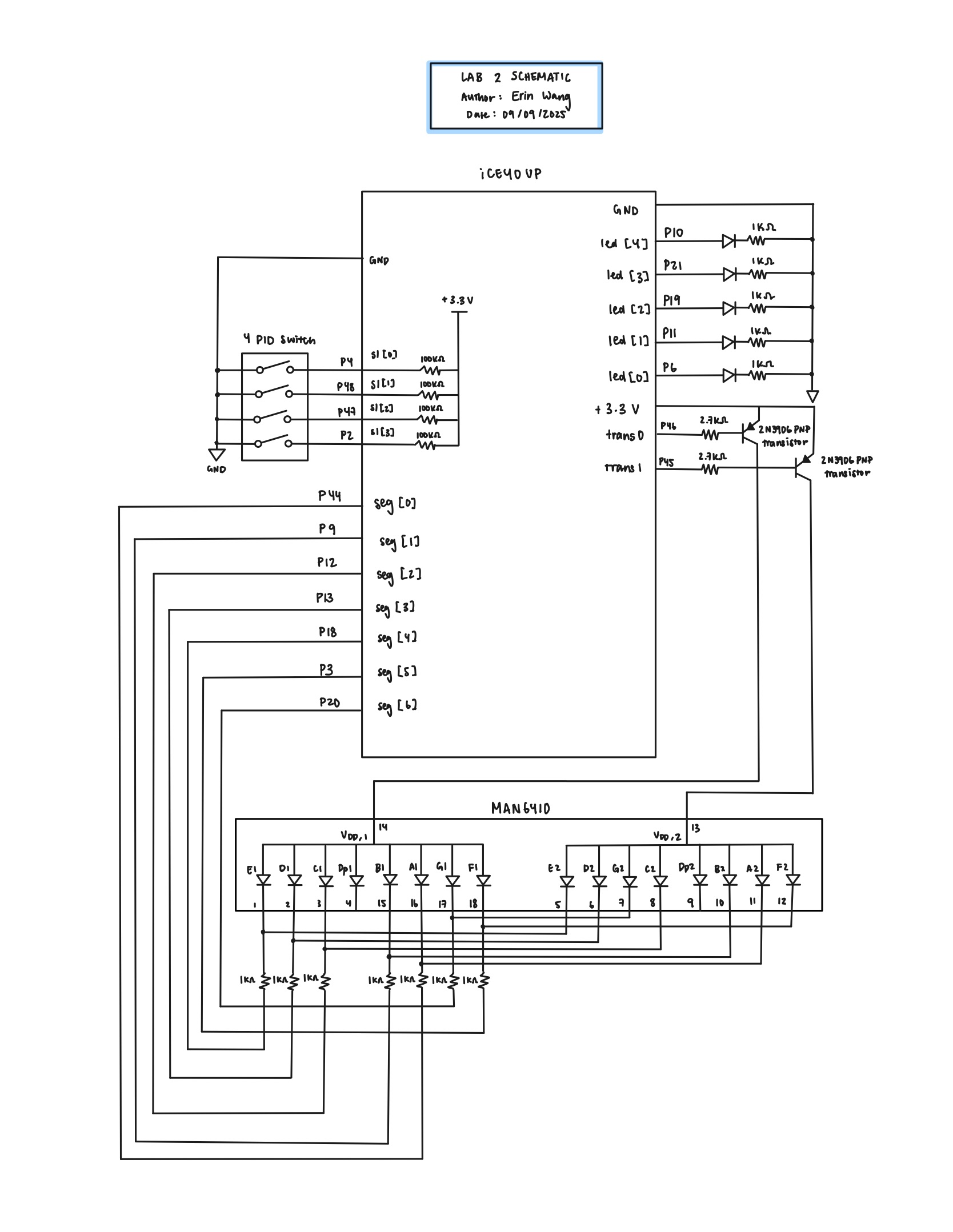
Figure 6 shows the physical layout of the design. An internal 100 kΩ pullup resistor was used to ensure the active low reset pin for the switches was not floating. The output 7-segment diodes were connected using a 1kΩ current-limiting resistor to ensure the output current (~1.4 mA) did not exceed the maximum output current of the FPGA I/O pins. The external LED diodes (green) were connected using a 1kΩ current-limiting resistor to ensure the output current (~1.4 mA) did not exceed the maximum output current of the LEDs. The figure also shows which pin number of the dual display corresponds to which segment (i.e. A1,A2,B1, B2…) of the 7-segment display.

Figure 7 depicts the assignment of letters to a digit of the output display. In the program, seg[0] corresponds to a, seg[1] to b, and so on.
Results and Discussion
Testbench Simulation
top Module

The design met all intended design objectives. Figure 8 shows a screenshot of the QuestaSim simulation for the top module’s testbench tb_top after approximately #10000 time units to show that the HSOSC toggles.

As shown in Figure 9, the simulated outputs of led match the ledexpected output. Note that not all the tested inputs of led are shown in this image. The outputs of top: seg, trans0, and trans1 are not tested in this testbench because they rely on the mpx module which uses the HSOSC clock to provide the transistor output and switch input into sevseg. The outputs for seg are tested in the sevseg testbench while trans0 and trans1 and the switch input into sevseg are tested in the mpx testbench.
sevseg Module

Figure 10 shows a screenshot of the QuestaSim simulation for the sevseg module’s testbench tb_sevseg. The simulated outputs of seg match the expected outputs.
mpx Module

Figure 11 shows a screenshot of the QuestaSim simulation for the mpx module’s testbench tb_mpx to test that the s, trans0, and trans1 output matches the expected outputs for before the alternation (aka flip) at counter = 200000. Because we are before the flip, s should be the same as the s0 input and trans0 and trans1 should be 0 and 1 respectively. The simulated outputs of mpx match the expected outputs for before the flip and the counter is counting up.

Figure 12 shows a screenshot of the QuestaSim simulation for the mpx module’s testbench tb_mpx to test that the s, trans0, and trans1 output matches the expected outputs for after the alternation (aka flip) that should occur when the counter reaches 200000. Because we are after the flip, s should be the same as the s1 input and trans0 and trans1 should be 1 and 0 respectively. The simulated outputs of mpx match the expected outputs for after the flip and the flip happens when the counter reaches 200000. The reset of the counter after count reaches 200000 is also visualized.
Conclusion
The design successfully displayed two individual digits on the dual 7-segment display using only one sevseg module. The 5 LEDs also successfully display the sum of the two inputs. There is no bleeding between the digits or flickering and the 7-segment display does not dim depending on which numbers are displayed. The digits are also upright to the viewer.
AI Prototype and Reflection
Without Lab 1 Files Provided
Off the bat I already recognized the Claude Ai put multiple modules in one file and the testbench module in another file. When trying to synthesize the code, there was an error in the testbench module. The testbench had two initial statements. The first initial statement housed the error of loop count limit exceeded forever never breaks. This is because the AI had setup the clock with the following code:
initial begin
    clk = 0;
    forever #5 clk = ~clk;
end
This block of code is notably different from how I implement a clock. I use an always statement instead of initial to setup the clock.
Just attempting to synthesize without including the testbench in implementation does work! Looking at theseven_seg_decoder module from the AI, the case statement looks like mine, accomodating for the common anode by having 1 as LOW and 0 as HIGH for the display. There is however no default case which could be a problem for debugging. The seven_seg_mux module uses the same clock divider setup as the provided example on the E155 website by using a counter and setting the multiplexer’s select to the last bit. What’s more strikingly different is that the input multiplexer code is an always_comb statement whereas I used the syntax for a multiplexer of select ? in1:in0. The AI also used an always_ff statement for the output demultiplexer with latches by turning the output to either all segments off or all segments on. However, we were told explicitly not to use latches and to use PNP transistors to control the anode power.
With Lab 1 Files Provided
With the Lab 1 files provided, the AI did not provide a testbench. The code was much shorter than without the Lab 1 files. The code does use HSOSC immediately which is different from the Lab 1 AI Prototype. For the time multiplexing, the AI created a clock divider to toggle at 1200 Hz. This seems a little high to me as a computer screen is around 60 Hz. Such high frequency could cause some bleeding between digits. The code for the multiplexer select is how I did the select in my code where the counter resets and the mux select switches to its opposite logic after a certain number of counts. The input multiplexer code was still an always_comb statement rather than the select ? in1:in0 format. The code then uses my sevensegment module to input the switch chosen from the always_comb statement and outputs the segments to turn on. The AI this time uses an always_comb for the output demultiplexer to use the multiplexer select from the clock divider to choose whether to make the first digit active and the second display off or vice versa. The default display is that both displays are off.
The code also provides a small section to use LEDs to check which display is active, check when the two inputs differ, and to blink at the frequency of the clock divider.
Overall, I think both codes are very high quality although may be a little wordy considering mux logic can be much shorter than an always_comb statement. The code was interesting to compare as we didn’t specify to the AI to send an output to PNP transistors to control which digit was on and I think the prototype had a clever way of sending the output to the LED segments.