Lab 3 Report
Lab Hours
I spent 60 hours on this lab.
Introduction
Lab 3 involved learning how to synchronize asynchronous inputs from a 4x4 keypad and use FSMs for memory to display the most recent input from the keypad as the right digit of a dual 7-segment display and the last input as the left digit.
Design and Testing Methodology
Dual Display with one 7-Segment Module
In order to display two independent hexadecimal numbers on the dual 7-segment display using only one sevseg module, the trick was to send the same output to both digits but alternate between turning on the first digit and the second digit fast enough that the different digits are seen at the same time to our eyes (~60 Hz). To alternate between the two, the on-board high-speed oscillator (HSOSC) from the iCE40 UltraPlus primitive library was used to generate a clock signal at 24 MHz then a counter was used to divide the high frequency clock signal into a 60 Hz signal.
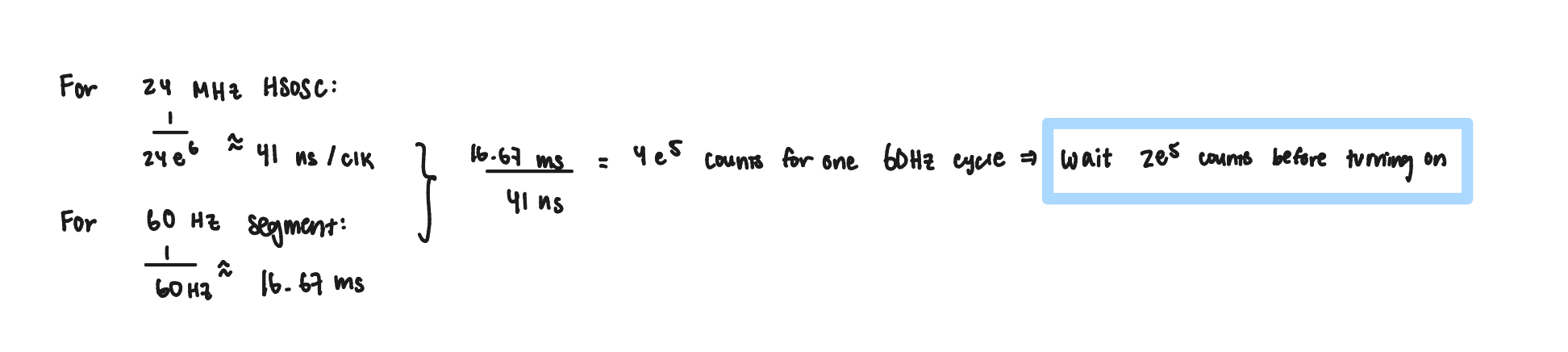
The calculation in Figure 1 derived that the counter needed to reach 200000 before setting the multiplexer select HIGH in order switch between the two inputs and turning on the two outputs at 60 Hz. For example, if the first digit should read 1 and then second digit should read 5, then when clk is LOW, the program takes 1 as the input and sends 1 to both digits’ outputs. Then, the program turns only the first digit’s power on and turns the other digit’s power off. When clk is HIGH, the program takes 5 as the input and sends 5 to both digits’ outputs. Then the program turns the second digit’s power on and turns the first digit’s power off. This switch happens fast enough that the human eye sees both individual digits on the display.
Resistor choice for 7-segment Display
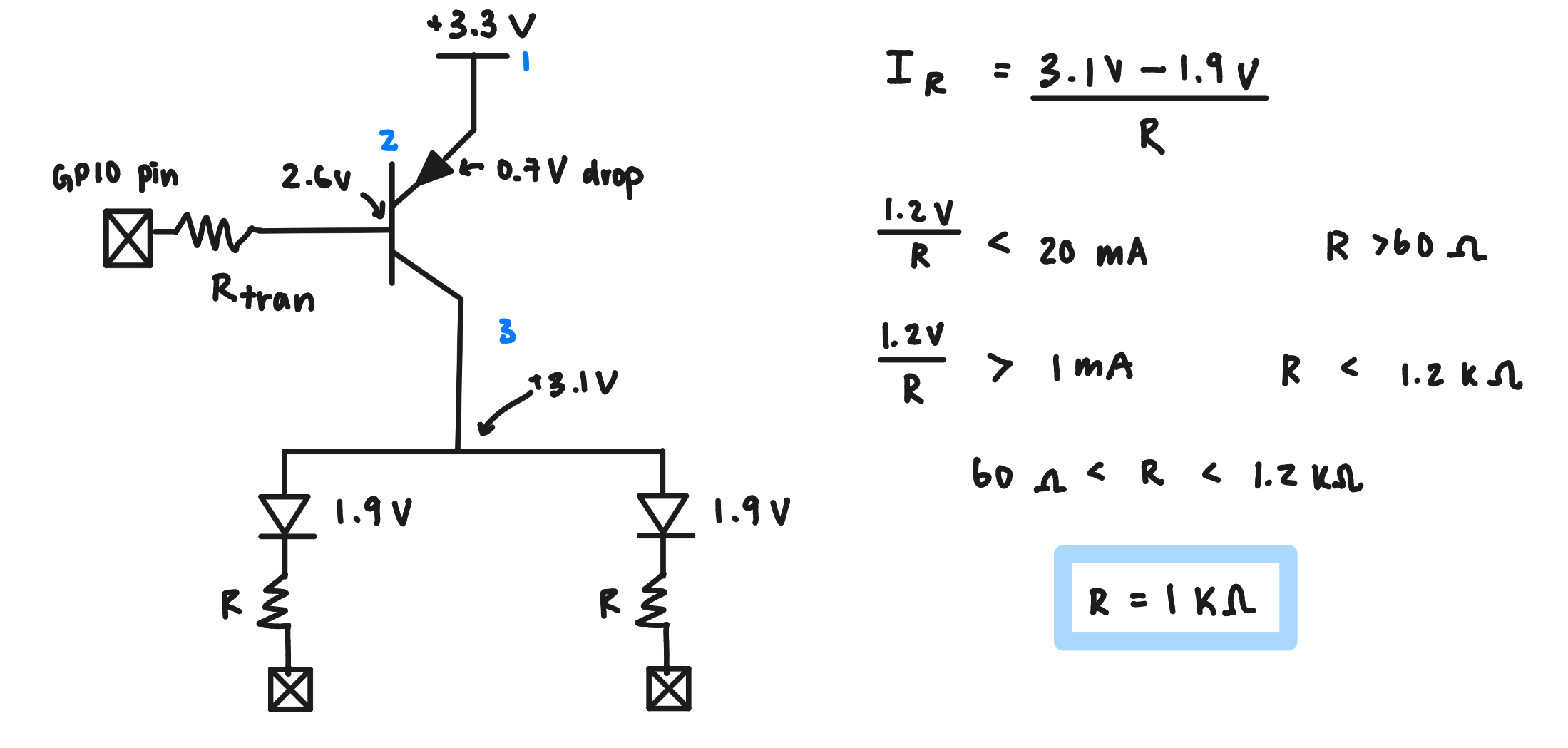
The calculation in Figure 2 derived 1kΩ as an appropriate resistor to provide ~1.2 mA to the LED segments of the 7-segment display. The drop in voltage from the emitter is due to the emitter saturation voltage. Thus the voltage going into the segment displays is 3.1 V.
Resistor choice for transistors
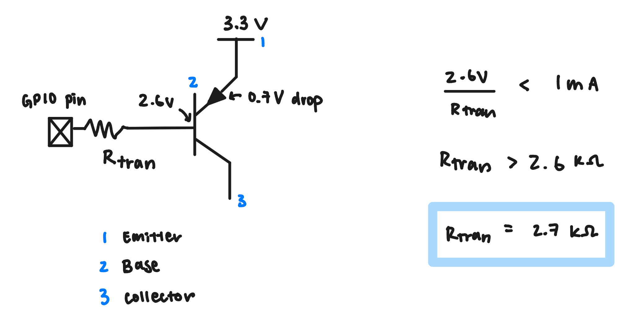
The calculation in Figure 3 derived 2.7kΩ as an appropriate resistor (stock-room available) to provide less than 1 mA to FPGA I/O pins.
Resistor choice for keypad inputs
In order to read the keypad keys, I chose to have my columns as one of my top module’s outputs. This means my program drives power to the columns and checks the rows for a press. I also chose to implement an active HIGH keypad, which means I needed pulldown resistors for the row inputs such that when there is no activity, the rows read 4'b0000. I chose 680Ω as the resistors to be large enough so as to not draw too much current from the FPGA pins and small enough to quickly pull down the signal and act as a pulldown resistor.
Debounce design and FSM diagrams
One of the mechanical issues with the keypad buttons is that the buttons “bounce” when pressed. I chose to debounce my keypad buttons using an 3-state FSM that waits for a button to be pressed, then when the button was pressed the FSM would enter a state that waits for a counter to reach high enough that the button would have stabilized, then when the counter reaches a set number the FSM would enter a state that waits for the button to be released.
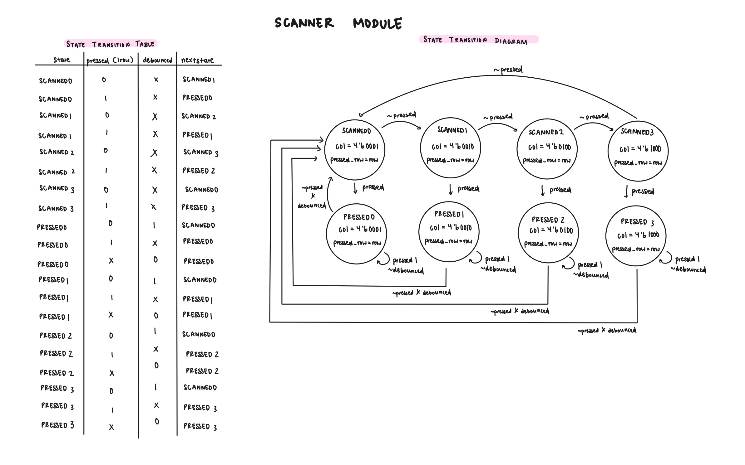
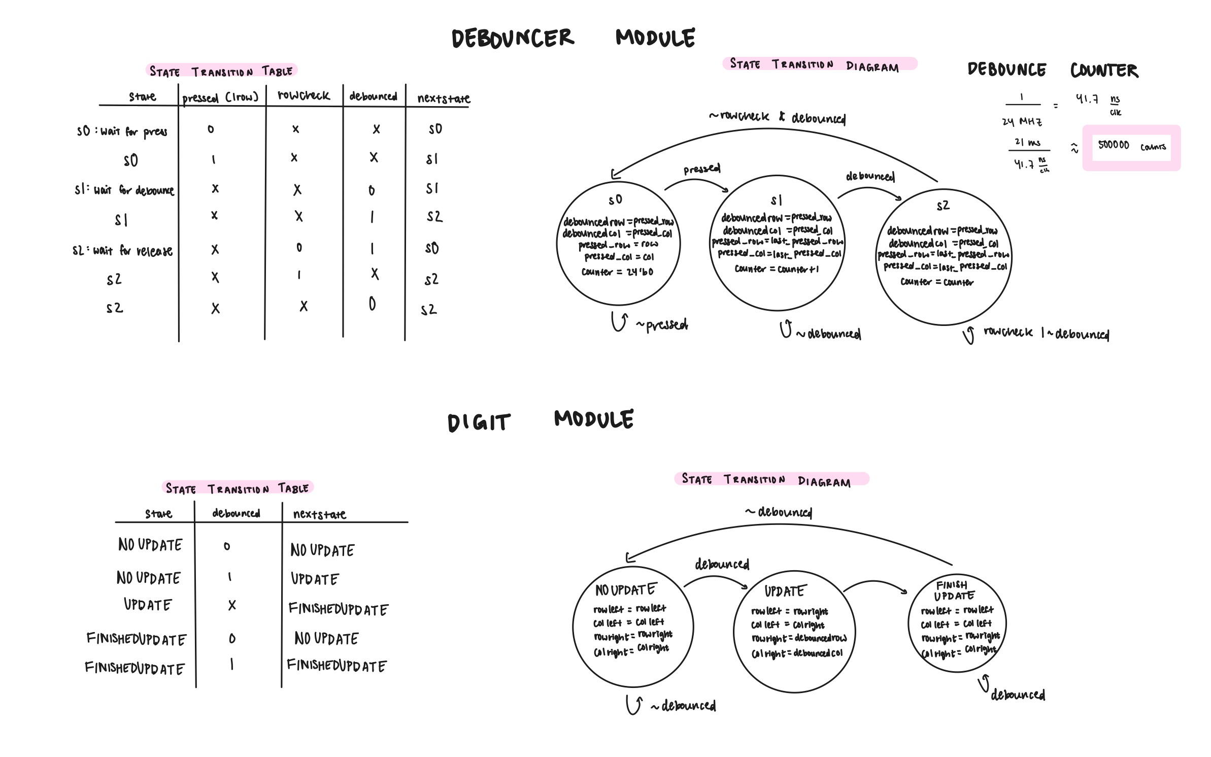
The images above detail the design of the three FSMs that I used in my overall implementation. One FSM was to switch between scanning for rows and holding when a key was pressed (Figure 4). Another FSM was the debouncing FSM to only register the keypress once (Figure 5). And the digit FSM was for switching between updating the digits and not updating the digits (Figure 5). The FSM is a simple strategy to store an input in “memory” and use this memory to decide what to do at the next clock cycle. However, some of the tradeoffs with the FSM is that the inputs and timing can get really tricky especially in this lab where multiple FSMs needed to communicate with each other.
Technical Documentation
The source code for the project can be found in the associated Github repository
Block Diagram
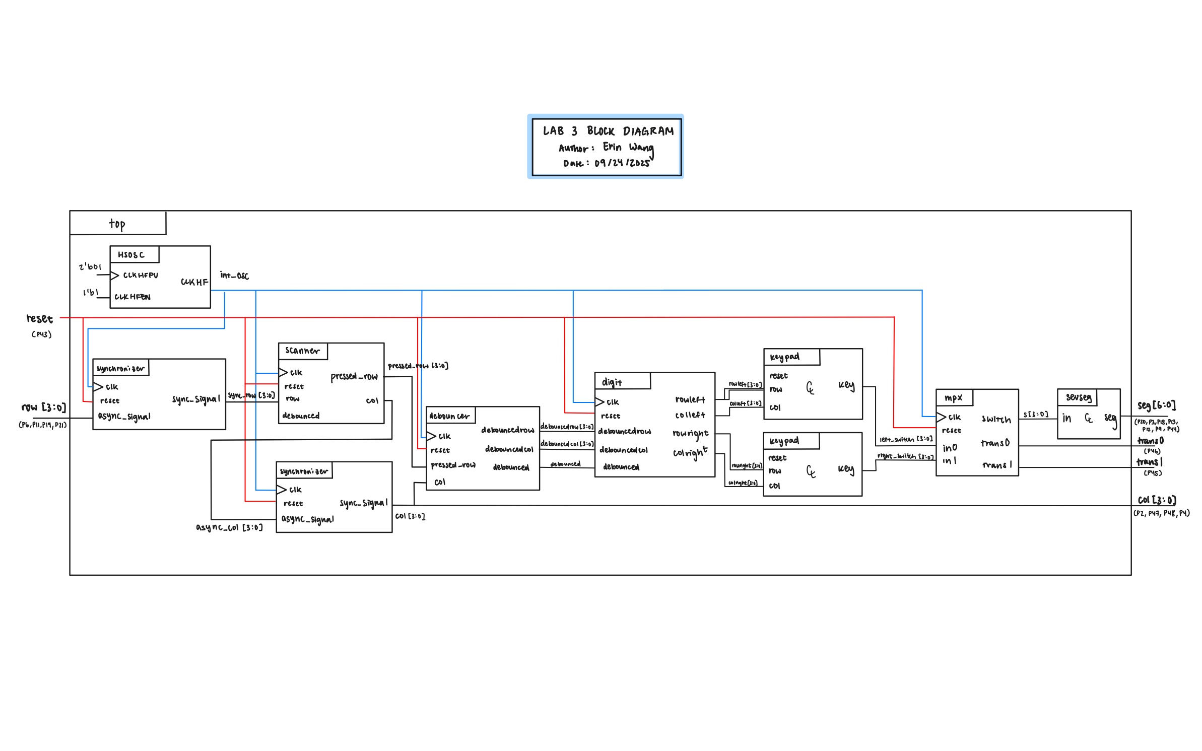
HSOSC, scanner, debouncer, synchronizer, digit,keypad,mpx, andsevseg`.
The block diagram in Figure 6 demonstrates the overall architecture of the design. The top-level module top includes 8 submodules: the high-speed oscillator block (HSOSC), the scanner to check for keypad presses, the debouncer to debounce the button presses, the synchronizer to synchronizer the row and col signals, the digit module to send the debounced signal either to the right digit and send the previous right digit to the left digit, the keypad module to decode a row and col pair into a key on the keypad, and finally the multiplexer to alternate at 60 Hz (mpx) and the 7-segment display module from Lab 1 (sevseg).
Schematic
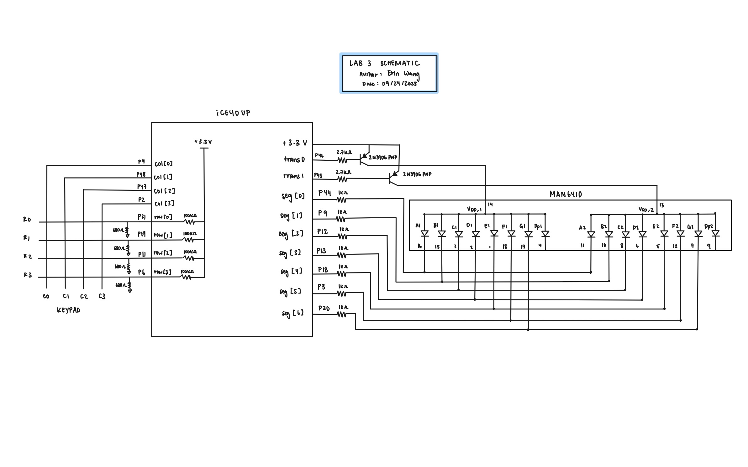
Figure 7 shows the physical layout of the design. The output 7-segment diodes were connected using a 1kΩ current-limiting resistor to ensure the output current (~1.4 mA) did not exceed the maximum output current of the FPGA I/O pins. The figure also shows which pin number of the dual display corresponds to which segment (i.e. A1,A2,B1, B2…) of the 7-segment display.

Figure 8 depicts the assignment of letters to a digit of the output display. In the program, seg[0] corresponds to a, seg[1] to b, and so on.
Results and Discussion
Testbench Simulation
top Module (HSOSC implied)

The design met all intended design objectives. Figure 9 shows a screenshot of the QuestaSim simulation for the top module’s testbench tb_top. Because all the outputs depend on HSOSC it can be assumed that HSOSC toggles. As shown in Figure 9, the simulated outputs of seg change when expected in relation to the led0 which holds the value for whether the button is debounced and counter from the mpx module which updates what key to send to the seg module. seg is expected then to change after the button is debounced (db/counter reaches 500000) and the mpx sends seg the key to output (db/mpx reaches 200000). I wrote tests for all 16 keys that seg matches expected for when the button is pressed, when another button is pressed while the first one is still pressed, and when the button is released. Although not pictured, the testbench passed all tests for all 16 keys.
scanner Module
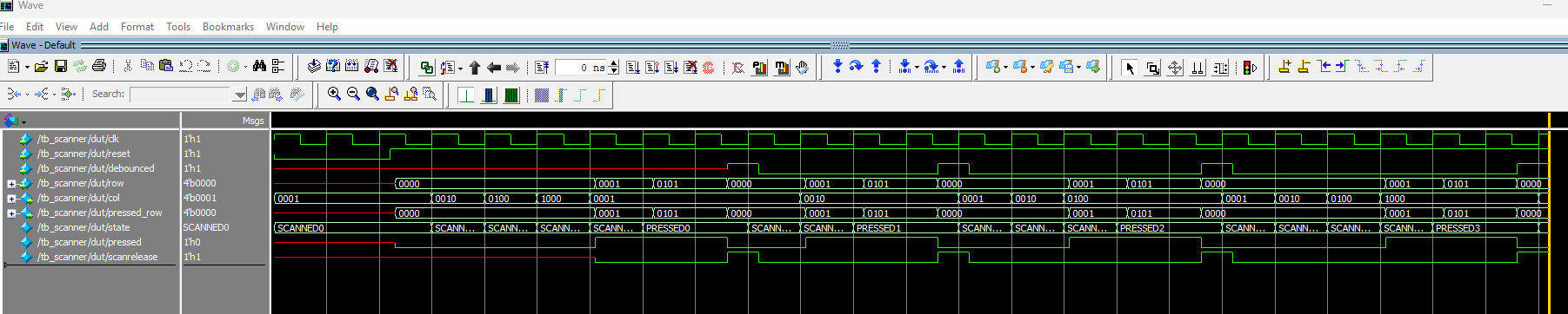
Figure 10 shows that the scanner module reaches all scanning states when no row is input and reaches all pressed states when a row is input at the corresponding column. At the end of the simulation, the image shows that the scanner module also correctly stays in the PRESSED state even when a new input key is pressed while the first key is held.
debouncer Module
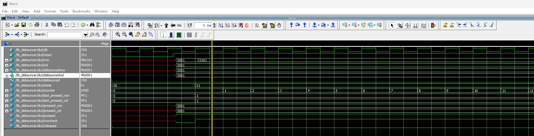
Figure 11 shows that the debouncer module moves from S0 (waiting for key press) to S1 when a key is registered and correctly stays in the S1 state of waiting for debounced to go high (counter to reach 500000) even when a new input key is pressed while the first key is held.
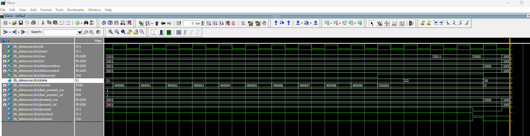
Figure 12 shows that the debouncer module moves from S1 (waiting for debounced) to S2 when debounced goes high and stays in the S2 state of waiting for the button to be released even when a new input key is pressed while the first key is held. The FSM also correctly moves back to S0 when the button is released (row input is 4'b0000). debounced also correctly goes high after the counter counts up to 500000.
synchronizer Module

Figure 13 shows that the synchronizer module correctly transfers the asynchronous input to the synchronized output after 4 clock cycles. The choice of 4 clock cycles was for the synchronized output to match the right SCANNING state in the scanner module, and there are 4 scanning states to run through in the scanning cycle.
digit Module

Figure 14 shows that the digit module visits all 3 states. The module correctly does not transfer any information when in the NOUPDATE state and correctly transfers the most recent input only to the right row/col and updates the left row/col with the previous values of the right row/col in the UPDATE state. The module also correctly only updates the right and left rows/cols by moving to the FINISHEDUPDATE state after updating once as well as returns to NOUPDATE when the debounced signal goes back to 0 (debouncer module is back to waiting for a button to be pressed).
keypad Module

Figure 15 shows that the keypad module correctly matches a row and column pair to its corresponding key on the 4x4 keypad.
sevseg Module

Figure 16 shows a screenshot of the QuestaSim simulation for the sevseg module’s testbench tb_sevseg. The simulated outputs of seg match the expected outputs.
mpx Module

Figure 17 shows a screenshot of the QuestaSim simulation for the mpx module’s testbench tb_mpx to test that the s, trans0, and trans1 output matches the expected outputs for before the alternation (aka flip) at counter = 200000. Because we are before the flip, s should be the same as the s0 input and trans0 and trans1 should be 0 and 1 respectively. The simulated outputs of mpx match the expected outputs for before the flip and the counter is counting up.

Figure 18 shows a screenshot of the QuestaSim simulation for the mpx module’s testbench tb_mpx to test that the s, trans0, and trans1 output matches the expected outputs for after the alternation (aka flip) that should occur when the counter reaches 200000. Because we are after the flip, s should be the same as the s1 input and trans0 and trans1 should be 1 and 0 respectively. The simulated outputs of mpx match the expected outputs for after the flip and the flip happens when the counter reaches 200000. The reset of the counter after count reaches 200000 is also visualized.
Conclusion
The design successfully read inputs from the 4x4 keypad and displayed the most recent input on the right digit of a dual 7-segment display and the last input on the left digit. The design does not lock up when multiple buttons are pressed. Each button press is only registered once and the 7-segment displays are the same brightness. The design has no latchesor tristate buffers. The design also uses synchronizers and only registers the first button press if additional buttons are pressed down while holding down one button. There is no bleeding between the digits or flickering and the 7-segment display does not dim depending on which numbers are displayed. The digits are also upright to the viewer.
Overall a success!
AI Prototype and Reflection
Prototype A: Monolithic Prompt
The Claude AI produced a code with 4 modules: a keypad_top module that drives columns and checks rows, a clk_divider module that is used both for scanning and display,a keypad_scanner module that jumps from scanning the different columns to a key-hold state to a key-release state, and a display controller with time multiplexing to alterante between the digits of the disp_clk rate and also holds the 7-segment decoder of what segments to activate on the display. The code actually synthesized on the first try which suprised me. Usually it takes a couple errors fed back into the AI to get a synthesizable code. Something that was interesting to me was that the code in the keypad_scanner module saved the pressed key as an array with the active column and the input low row. I also thought that later in the same module, the output register had a really interesting implementation of having a variable holding whether the key is valid that relies on whether the next state is the KEY_RELEASED state.
Prototype A Scanner Register Code
always_ff @(posedge scan_clk or negedge rst_n) begin
        if (!rst_n) begin
            key_code  <= 4'h0;
            key_valid <= 1'b0;
        end else begin
            key_valid <= (next_state == KEY_RELEASED);  // Pulse on key release
            if (key_detected && (state != KEY_HELD)) begin
                key_code <= pressed_key;
            end
        end
    end
I thought this was an interesting implementation since I’ve always been taught to put this kind of logic in an always_comb and to add more states if needed rather than to put the logic in the flop register. I didn’t use active-low in my design, but I heard many people had issues with getting one of the specs of holding down one button then pressing another button in the same column (if driving columns and checking rows) then releasing the first button and keeping the second button pressed and registering the second button once. The idea of a key_valid in the flop could possibly circumvent this, but it’s hard to check without having an active-low hardware implementation to test on.
There were way less FSMs than in my implementation. The keypad_scanner module also used the slowed down clock from clk_driver to work the FSM state register. I believe this was to address the problem of debouncing which was different from my implementation of using an FSM.
Prototype B: Modular Prompts
This time the Claude AI produced 3 modules: keypad_top, keypad_scanner, and keypad_oneshot. However, the design did not synthesize due to the use of the SB_HFOSC module which we are not using. This was an issue I’ve run into in the first lab AI prototype. After telling the AI to use HSOSC instead, the code ran into another issue of instantiating unknown modules for sevenSegment. Feeding this into the AI caused the AI to build the module which then allowed the code to synthesize!
The debounce FSM was actually very similar to my own FSM with an IDLE, DEBOUNCE, KEY_HELD, and WAIT_RELEASE state. I actually ended up only using three states for idle, waiting for debounce, and waiting for release. In terms of synthesizability, the modular prompts needed more help and guidance to produce a synthesizable code. Because I’m more familiar with FSM structure, it was a little easier to follow than the monolithic prompt. However, the size of the code with so many FSMs does mean the readability decreases a bit. This could also be in part due to having all the modules on the same file. I had a lot of timing issues in my own code while debugging, and what I see with this code is that a lot of the variables that deal with FSM states are computed internally in the module when possible as opposed to grabbing the necessary input from other FSMs. The modular prompt also caused the clock dividing to be placed in the keypad_top module rather than in a separate clk_divider module which also reduced readability.